Framed registers
Traditional CPU architectures integrate their registers directly into the microchip for the fastest possible access. By contrast, regular memory is located in separate microchips, which the CPU accesses using a memory bus.
Chombit introduces a novel concept called framed registers which are mapped to main memory and therefore also accessed via the bus. This means that the framed register has a memory address, a key difference from Chombit's conventional registers. Because bus access is slower, this is an inefficient design from an electronics perspective, however it facilitates learning by eliminating the assembly language bookkeeping that is typically required to move variables in and out of registers. Framed registers also simplify the effects of a compiler, making it easier to understand how source code corresponds to assembly code.
Despite these simplifications, from an educational perspective Chombit's architecture nonetheless preserves the character of a real CPU. Unlike an interpreted bytecode or intermediate language, each Chombit instruction represents an atomic operation that can be understood as a digital circuit. Each instruction has a predetermined clock cycle cost and operates directly on a traditional memory bank without any abstractions.
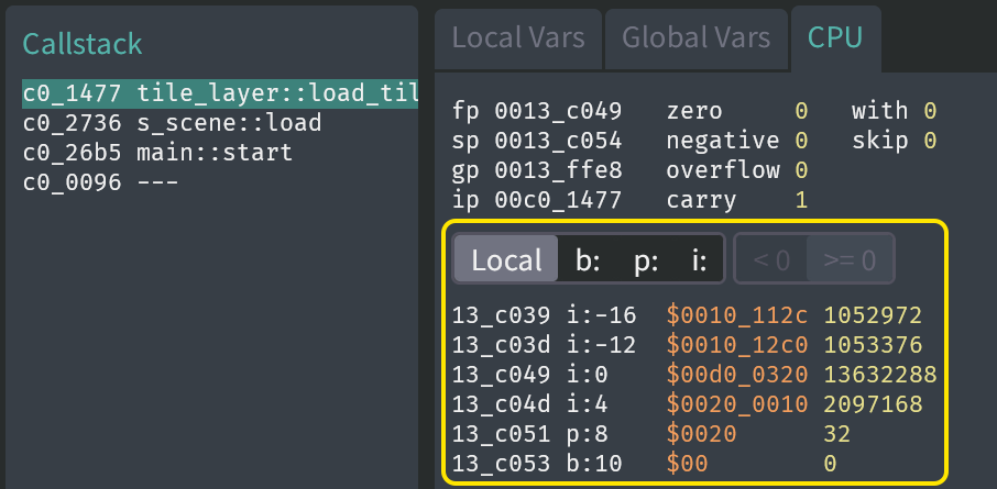
Debugger view
The Hybrix debugger displays the framed registers in the lower part of the CPU tab, with two view options:
localshows only the framed registers used in the currently active function (as determined by the debugger's symbol table, if available)b:,p:, ori:shows all possible indexes for a given framed register size
Details
Consider the following CPU instruction, which uses two framed registers p:-7 and i:12:
c0_0000: e6 f9 03 56 78 load p:-7, [i:12 + $5678]
Technical points:
-
The register name has a register size prefix
b:,p:, ori:that indicates its storage sizebyte,pair, orint. -
The machine language opcode byte (
$e6in the above example) encodes the instruction kind (load) as well as its register sizes. Here is how it appears in theloaddocumentation:Opcode Bytes Cycles Form $e6 5 4 load p:_, [i:_ + {s_pair}] -
A register name has a register index suffix that is a signed decimal integer. For example, in
p:-7, or ini:12. -
The operand byte encodes the register index using two's complement with a range from (
$c0) to ($bf). -
For negative indexes, the operand byte is the two's complement of the index value. For example, becomes
$f9in hexadecimal in the above example. -
For positive indexes, the operand byte divides by the register size. For example, if our framed register is
i:12, then divides by bytes (forint) to produce$03in hexadecimal. -
This means that positive indexes must be a multiple of the register size. For example, we can have
p:66(a multiple of ), whereasp:67andi:66are impossible. -
The notation
{s_pair}simply means an literal (immediate) value that is a signed 16-bit integer, using decimal or hexadecimal syntax.The table below summarizes the ranges of possible register indexes:
Storage size Minimum Maximum byteb:-64b:191pairp:-64p:382inti:-64i:764 -
Modeling negative/positive indexes this way accommodates the Hybrix calling convention, where positive indexes represent local variables (numerous and easily reordered), whereas negative indexes represent function parameters (limited number and fixed order).
-
The register's storage address is computed by adding FP to the register index. For example, if FP is
$0010_0009thenp:-7refers to$0010_0002, andi:12refers to$0010_0015(because which is$15in hexadecimal). -
Chombit always uses big-endian storage. For example, if FP is
$0010_0009and we store$abcdin the framed registerp:-7, then$abis written at address$10_0002, and$cdis written at$10_0003. -
Framed registers of different sizes can map to the same memory, in which case writing to one will alter the value of the other. For example,
i:4andp:6will have two memory bytes in common. Typically this produces memory corruption bugs, however it could be leveraged for advanced optimizations.